
| 原産地: | 中国(本土) | 銘柄: | hs | Min.線幅: | 0.1mm | 基材: | fr4 | 表面の仕上げ: | osphaslの浸金 | Min.行送り: | 0.1mm | 板厚さ: | 0.8〜1.6ミリメートル | Min.穴のサイズ: | 0.2mm | 銅の厚さ: | 1-5oz | pcbのクローン: | 許容 | 層の数: | 1-14layer | その他のサービス: | 購入およびassambleコンポーネント | はんだマスク: | 白、 黒、 緑、 青、 赤、 等。 | dsignサービス: | 利用可能な | テスト: | 機能検査 | 配達: | /dhlフェデックス/ups/ems | 保証: | 2年 |
包装
| 包装: | 内側の真空パッキング、 外のカートンボックス |
We can do for you:
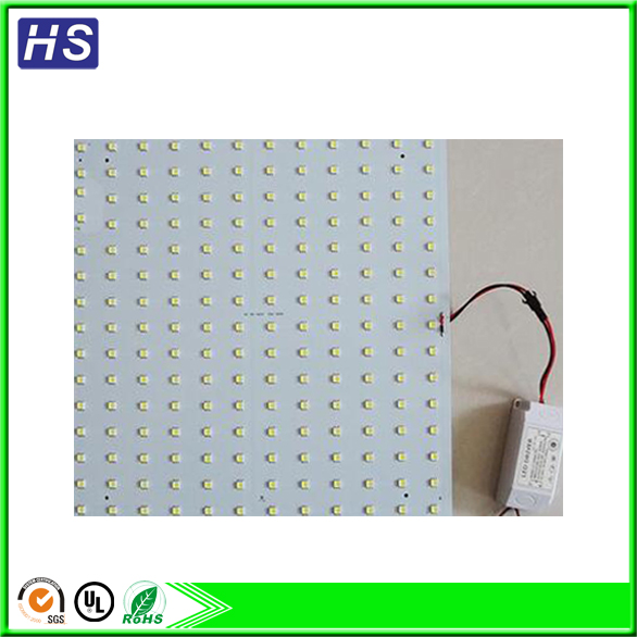
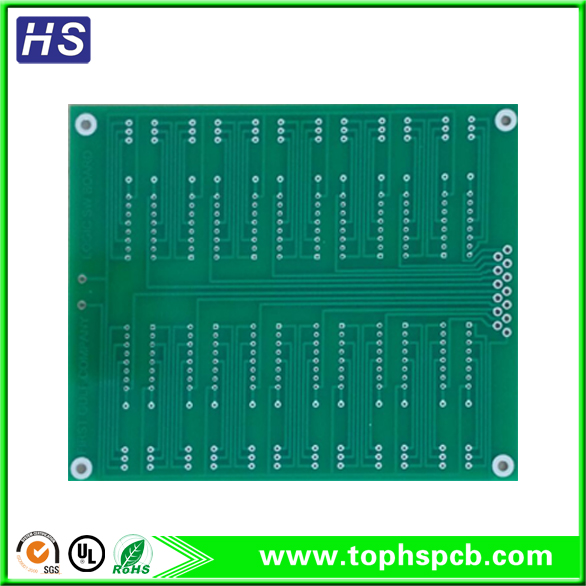
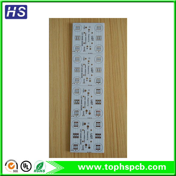
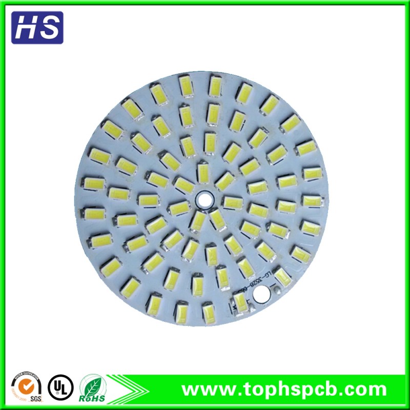
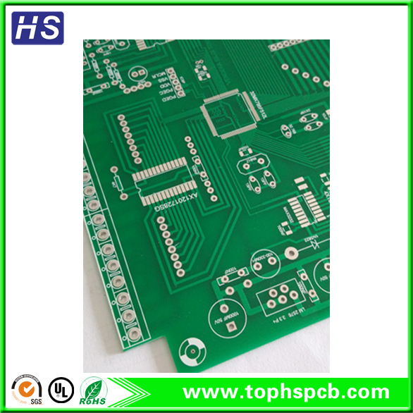
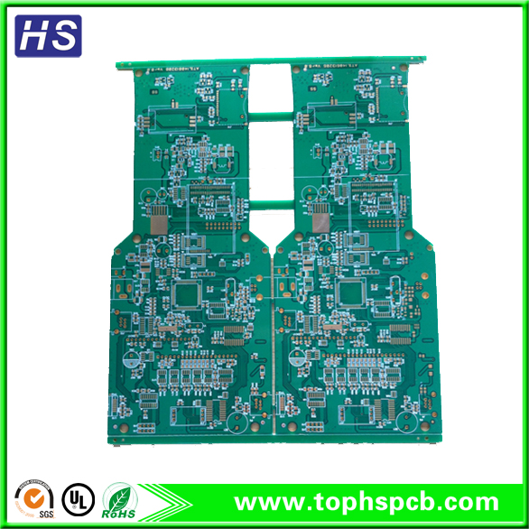
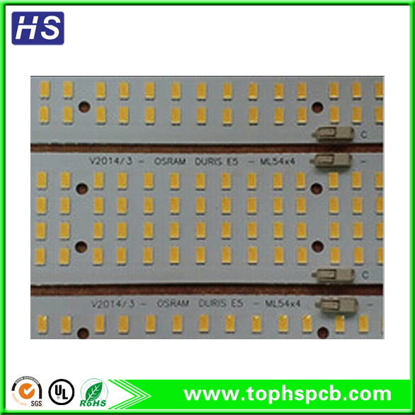
♦ 1—16 layer FR4 PCB,1—2 layer Aluminum PCB,Flexible PCB.
♦ 1—6oz copper thickness.
♦ 0.2mm hole size.
♦ 0.1mm line width/space.
♦ PCBA
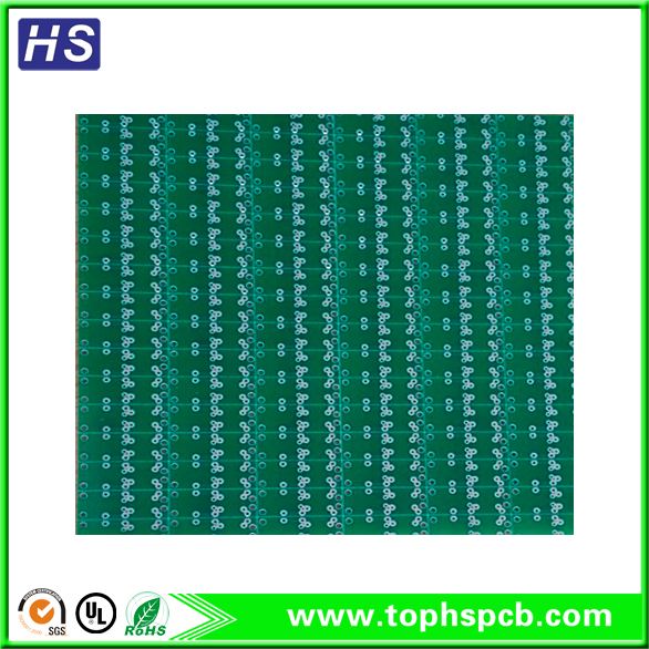
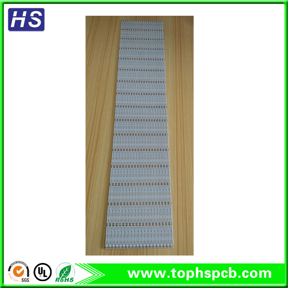
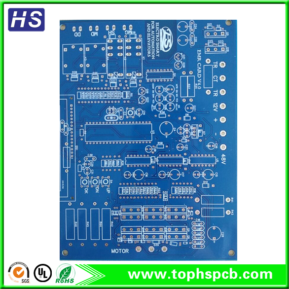
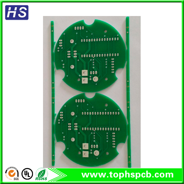
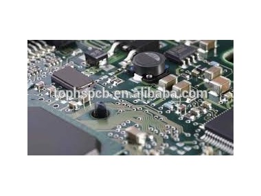
PCB for electronic products:
Our PCBs are used for wide range of products,such as WIFI,medical device,Tablet,Smart phone,e-Reader,Power supply,GPS,UPS,LED lights,etc.
Superiority
1.High efficiency&Experience
We can provide one stop service.Established in 2005, with many years hard-working and constant innovation,we have grown up into a professional PCB&PCBA manufacturer. We have our own independent research and development department and sophisticated quality control system.
2.Quality
Our product are manufactured according to the UL/Rohs standards to insure quality assemblies from start to finish. Whether it's a simple product or a complex turnkey production run, We will adhere to the highest quality standards.
3.Protecting your interests
Protecting your Intellectual Property is job one! Our staff of trained professionals are all working under a strict confidentiality contract and treat your important documentation as they would their own.
4.Service
We can provide 24hours service for you. We pride ourselves on our ability to custom tailor programs around our customers' needs.We take time to listen to your unique business needs and then set out to surpass them.
PCB quotation needs:
A. PCB GERBER file and specification .
B. Your special requirements for the PCB Board.
C. Your testing instructions if you wanna test.
Factory Manufacture Capability:
item | Manufacture Capability |
Material | FR-4/HiTg FR-4/Lead free Materials /CEM-3, Aluminium, metal based |
Layer No. | 1-16 |
Finished board thickness | 0.2 mm-3.8mm’(8 mil-150 mil) |
Board Thickness Tolerance | ±10% |
Cooper thickness | 0.5 OZ-11OZ (18 um-385 um) |
Copper Plating Hole | 18-40 um |
Impedance Control | ±10% |
Warp&Twist | 0.70% |
Peelable | 0.012"(0.3mm)-0.02’(0.5mm) |
Images | |
Min Trace Width (a) | 0.075mm (3mil) |
Min Space Width (b) | 0.1mm (4 mil) |
Min Annular Ring | 0.1mm (4 mil) |
SMD Pitch (a) | 0.2 mm(8 mil) |
BGA Pitch (b) | 0.2 mm (8 mil) |
Solder Mask | |
Min Solder Mask Dam (a) | 0.0635 mm (2.5mil) |
Solder mask Clearance (b) | 0.1mm (4 mil) |
Min SMT Pad spacing (c) | 0.1mm (4 mil) |
Solder Mask Thickness | 0.0007"(0.018mm) |
Holes | |
Min Hole size (CNC) | 0.2 mm (8 mil) |
Min Punch Hole Size | 0.9 mm (35 mil) |
Hole Size Tol (+/-) | PTH:±0.075mm;NPTH: ±0.05mm |
Hole Position Tol | ±0.075mm |
Plating | |
HASL | 2.5um |
Lead free HASL | 2.5um |
Immersion Gold | Nickel 3-7um Au:1-5u'' |
OSP | 0.2-0.5um |
Outline | |
Panel Outline Tol (+/-) | CNC: ±0.125mm, Punching: ±0.15mm |
Beveling | 30°45° |
Gold Finger angle | 15° 30° 45° 60° |
Certificate | ROHS, ISO9001:2008, SGS, UL certificate |
Shipment


Welcome to Hansion PCB factory