
| 原産地: | 中国(本土) | 銘柄: | sg | モデル番号: | SG-D016 | Min.線幅: | 0.075ミリメートル | 基材: | fr4 &ポリイミド | 表面の仕上げ: | enig | Min.行送り: | 0.075ミリメートル | 板厚さ: | 0.6ミリメートル-0.8ミリメートル | Min.穴のサイズ: | 0.2ミリメートル機械掘削と0.15ミリメートル用レーザー掘削 | 銅の厚さ: | 0.5オンス | pcb/fpcタイプ: | リジッドフレックスpcb | oem/odm: | フレックスリジッドプリント回路oem | pcb標準: | IPCII-6013 | 表面仕上げ: | hasl/ゴールド浸漬 | 認証: | ul、rohs、sgs | ·インピーダンスボード: | カスタマイズされた | はんだマスク: | イエロースクリーンカバーレイ/グリーンソルダーレジスト | 試験方法: | e-テスト | pcb/fpcサービス: | 剛性のフレキシブル回路基板設計 | 品質保証: | 12ヶ月 |
包装
| 包装: | bluetoothヘッドセットリジッドフレックスpcb: 1. accordingする買い手の要求2。インナー:抗静的バッグ+真空パッケージ3. outer:標準的な輸出カートン |
Product Description
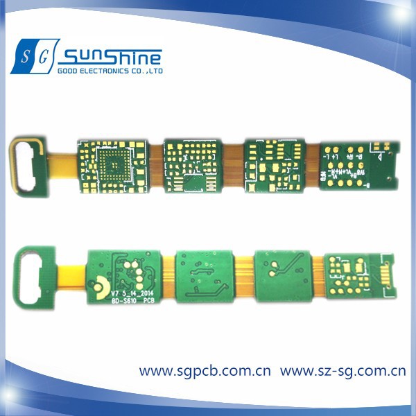
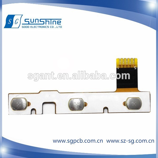
Layers of Bluetooth Headset R-FPCB: 4 Layers
Stack-Up of Bluetooth Rigid Flex Circuit: Solder Mask+Copper+FR-4+Glue+Coverlay+Copper+base Material+Copper+Coverlay+Glue+FR-4+Copper+Solder Mask
Headset R-FPCB Material: PI-Core Copper Sheet
Flex-Rigid Circuit Dimension: 63.8*10.4*0.57mm
Smallest Hole Diameter: 0.15MM
Minimum Track Width/Space :Minimum Track Width :0.1/Minimum Track Space:0.07
Surface Processing of Headset Flex-Rigid Circuit: Gold Immersion
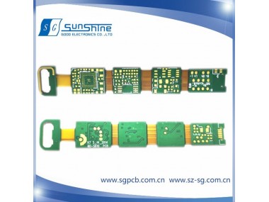
Features of Bluetooth Headset R-FPCB:
1. Small dimension with high circuit integration in design
2. Exclusively designed for Bluetooth headset with strict requirement towards the space dimension
3. High requirement towards the characteristic impedance to ensure smooth transference between input and output end
4. Adoption of special lamination technology to ensure the lamination reliability between the rigid board area and the flex board area
Fabrication Problems for Bluetooth Headset Flex-Rigid Circuit:
1. Deviation of the through holes caused by the extremely shrink of the flex board material
2. Disconnection between the flex area and rigid ara caused by wrong operations for buried vias
3. Unmatch characterisitic impedance caused by wrong operations in PCB etching procedure
Company Profile:Shenzhen Sunshine Good Electronics Company profile
Established in 2005, Shenzhen Sunshine Good Electronics Co., Ltd. initially focused on the flexible printed circuitboard
(FPC), the research and development of the Radio Frequency Identification (RFID). Currently, the Shenzhen Sunshine GoodElectronic Company Ltd has become a hi-tech private company that integrates product research and development,
product design, FPCB/RFID manufacturing, NFC project, PCBA processing and packing services, and product evaluation andanalysis. Therefore, Sunshine Good electronic Company can provide customs one-stop service.
PCB Technology
Specification of PCB Manufacturing | ||
1 | Description | PCB Specification |
2 | Material | FR-4/HTG150-180 FR-4/CEM-1/CEM-3/Aluminum |
3 | Layer | 1-28 |
4 | Board Thickness | 0.18mm- 4.0mm |
5 | Board Thickness Tolerance | +/-10% |
6 | Copper thickness | 17.5um-175um (0.5oz-5oz) |
7 | Min Trace Width | 0.15mm |
8 | Min Space Width | 0.15mm |
9 | Min Drilling Dia | 0.2mm |
10 | PTH copper thickness | 0.4-2mil(10-50um) |
11 | Tolerance of Etching | ±1mil(±25um) |
12 | V-cut angle | 25°,30°,45°,60° |
13 | Pearl Strength of line | ≥ 6lb/in(≥ 107g/mm) |
14 | Impedance control and tolerance | 50Ω±10% |
15 | Twist&Wrap | ≤ 0.5% |
16 | Soldermask | Green, Red, Blue, White, Black, Yellow |
17 | Surface Finish/Plating | HASL/Lead Free HASL/OSP/Gold Plating/Immersion Gold/ENIG |
18 | Certificate | ROSH. ISO9001, UL Certificate |
19 | File | Protel 99se/P-CAD/Autocad/Cam350 |
FPC Technology
Specification of FPC Manufacturing | ||
Items | Volume | Prototype |
Types | Single-sided, Double-sided, Multi- layers,Rigid-Flex circuit | Single-sided, Double-sided, Multi-layer, Rigid-Flex circuit |
Layer count | Flexible Circuit:1-8 Layer Rigid-Flex Circuit 2-8 Layer | Flexible Circuit:1-8 Layer Rigid-Flex Circuit 2-16 Layer |
Max Finish Board Size | 250*650mm | 250*650mm |
Board Thickness | 0.15mm -0.6mm | 0.15mm -0.6mm |
Min. Line Width/Spacing | 3mil3mil | 3mil3mil |
Finish Board tolerance | ±0.05mm | ±0.05mm |
Insulation layer thickness | 12.5um-50um | 12.5um or >50um |
PTH hole copper thickness | ≥0.01mm | ≥0.01mm |
Min NC drill hole diameter | 0.2mm | 0.2mm |
Laser drill hole diameter | 0.1mm | 0.1mm |
ENIG | AU:0.025-0.125um Ni:1-4um | AU:0.025-0.125um Ni:1-4um |
Electronic Nickle Immersion Gold | AU:0.025-0.125um Ni:1-5um | AU:0.025-0.125um Ni:1-5um |
Immersion Tin | Sn:0.025-0.125um | Sn:0.025-0.125um |
OSP | 0.1-0.5um | 0.1-0.5um |
HASL | 1-40um | 1-40um |
HAL | 1-40um | 1-40um |
Immersion Silver | ≥0.15um | ≥0.15um |
Impedance control | ±100% | ±100% |
Testing | Flying Probe Test,X-ray Inspection AOI Test | Flying Probe Test,X-ray Inspection AOI Test |