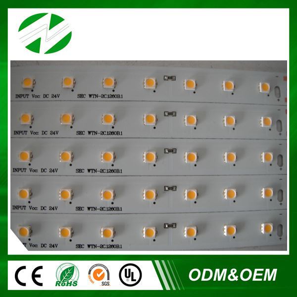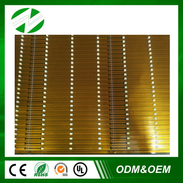

| 原産地: | 中国(本土) | 銘柄: | Zh-tec | モデル番号: | Zh-pcb | Min.線幅: | 0.1mm | 基材: | Fr-4 | 表面の仕上げ: | pcbaのために表面保護コーティング | Min.行送り: | 0.2mm | 板厚さ: | 0.2-5mm | Min.穴のサイズ: | 0.1mm | 銅の厚さ: | 1oz-3oz | type2製品: | 両面デザイン紫色はんだマスク基板 | pcb設計: | カスタマイズされた | pcbコピー: | に専門でコピー | pcb色: | 緑/黒/white/red/blue/yellow | pcbアセンブリ: | /oemodm |
包装
| 包装: | pcbaの破片でプラスチックesdバッグ、 その後pcbasカートンで |
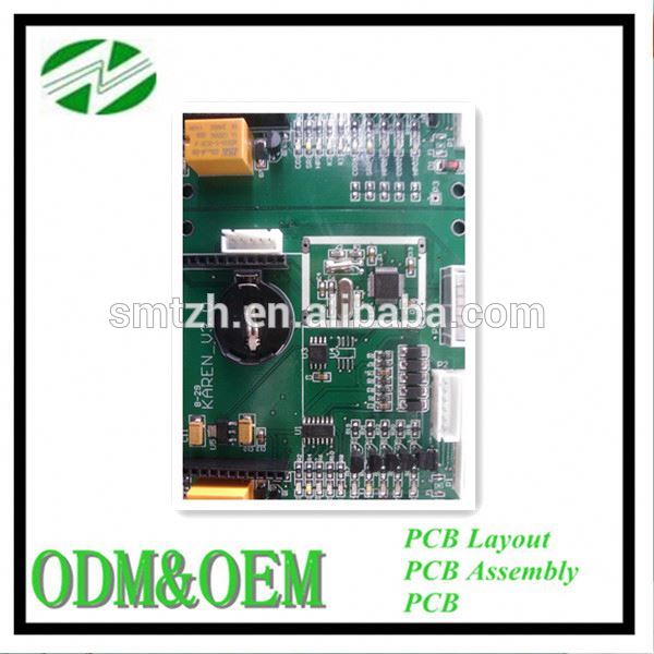
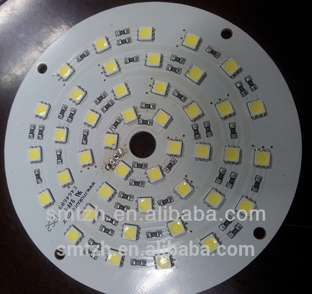
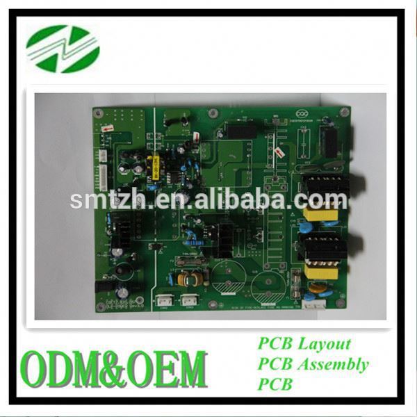
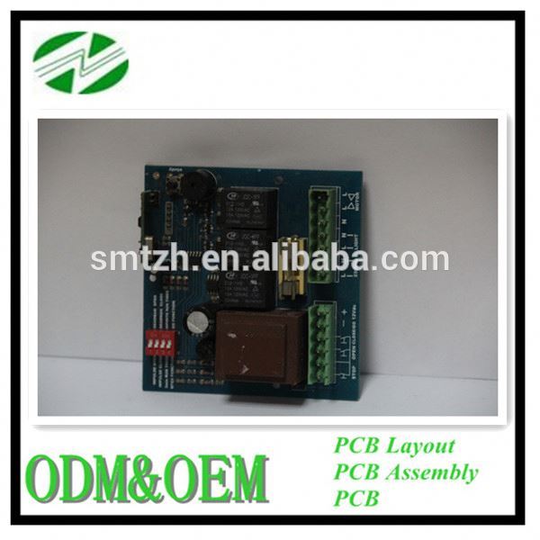
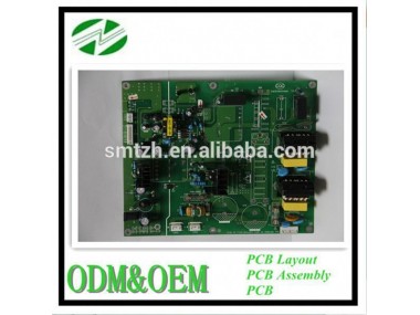
Electronic Digital Gold finger double sided purple solder mask pcb design
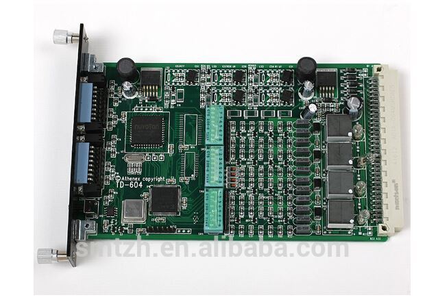
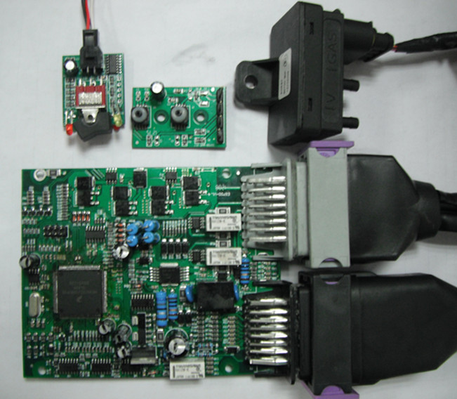
PCBA & PCB Assembly Manufacturer With Low Cost
We have much expereince in various of electrical product PCB design and assembly
- We provide PCB assembly turkey service,OEM and ODM
- Only BOM and Gerber file(PCB file) is needed
- Strong component sourcing capability to achive low price
- Production flow in accordance with technic and environmental requirment
- Have internal conformal coating process
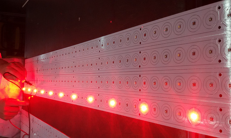
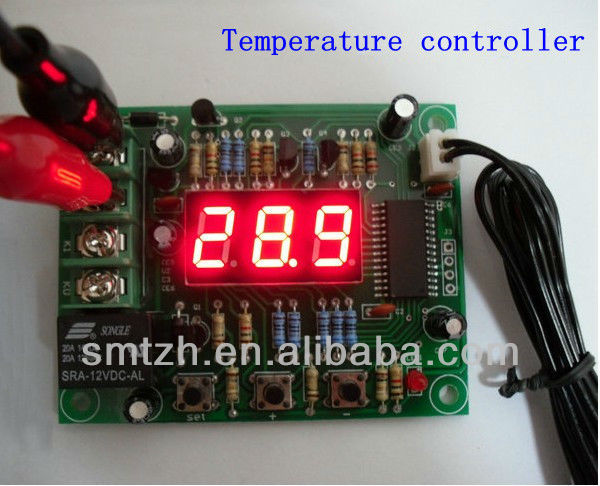
- Programmable logic controller(PLC) test fixture is utilized to test electrical function of PCBA
- 100% final test
- High quality ensured
Our SMT specification:
Quantity | Prototype&Middle &high volume PCB Assembly service are available |
Type of Assembly | SMT ,Thru-hole, Shell&molding assembly |
Solder Type | Leaded and Lead-Free |
Components | Passives Down to size 0201 ,BGA and VFBGA 0.025mil spacing, QFP |
Bare Board Size | Smallest:6mm*6mm Largest:1200mm*600mm |
File Formats | Bill of Materials Gerber Files, Bom list of components |
Type of Service | Turnkey service, Reply requirement in 12-24 hours |
Component Packaging | Cut Tape Tube Reels Loose Parts |
Lead Time | It depends on requirement ,usually for Prototype 5-10days, For bulk order15-45days |
Package | Anti-static bag, Foam protection ,Carton box |
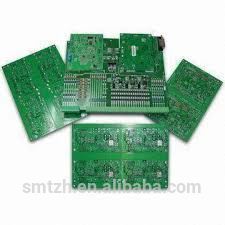
PCBA Making Process
Drilling-----Exposure-----Plating-----Etaching & Stripping-----Punching-----Electrical Testing-----SMT-----Wave Soldering-----Assembling-----ICT-----Function Testing-----Temperature & Humidity Testing
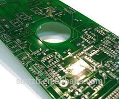
PCB Designs
Producing PCB boards based on schematic diagrams as provided by clients.
Producing PCB boards according to PCB diagrams furnished by clients. If applicable, adjustments or improvements in design meeting their requirements may apply.
Advantage to help customer reduce costs:
We have re-engineered numerous customer designs in addition to designing for manufacturing on our in-house engineering projects. Our comprehensive set of design guidelines can reduce costs and improve product quality through:
- Component selecion for process improvement
- PCB layout and construction analysis
Sensible components brand recommendation to get requirement
Comparative Advantage
- We provide comprehensive services in industrial designs, electronic designs, prototypes, mould-making etc.
- We have extensive experiences in R&D accumulated from handling hundreds of products in more than 10 categories.
- We have an excellent and robust R&D team focusing on R&D supplemented by conducting touchups and production.
Quotation requirement:
- PCB gerber file.
- Bom list of components /components list.( bom including components specification,package,quantity,item etc)
- For the IC ,if you need to burn software on ic ,you should get us software ,software model.
- If need function test or other requirement, just inform us at first time.
- If you don't have pcb file ,pls send sample to us
- Quantity required