
| 原産地: | 中国(本土) | 銘柄: | リード | モデル番号: | led pcb | Min.線幅: | 0.10ミリメートル | 基材: | アルミベース | 表面の仕上げ: | hal/osp/浸漬ゴールドメッキ/ゴールドメッキ/snメッキ/浸漬sn | Min.行送り: | 0.08ミリメートル | 板厚さ: | 0.6〜3.0ミリメートル | Min.穴のサイズ: | 0.2ミリメートル | 銅の厚さ: | 0.5オンスの6オンス | 色: | 白黄色 | 他のサービス: | pcbでledアセンブリサービス | 基準: | ul & rohs | サービス: | oem & odm | 層: | 1-16layers | combustibility: | 94v0 | 特別な技術: | bgaことが2.5mil、絞り(最小) 0.075ミリメートル、mid | 耐圧: | 2-4.5ボルト | 熱伝導率: | 1.0-370ワット/mk |
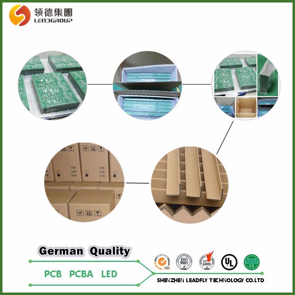
包装
| 包装: | 真空パックと箱に入れて |
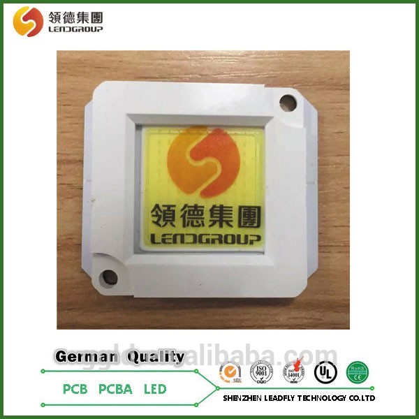
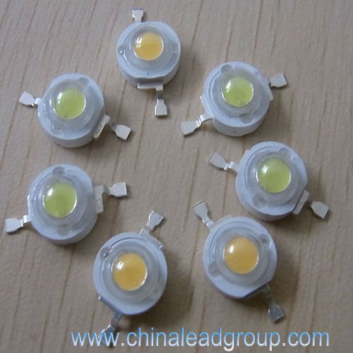
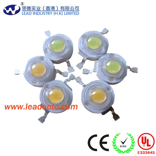
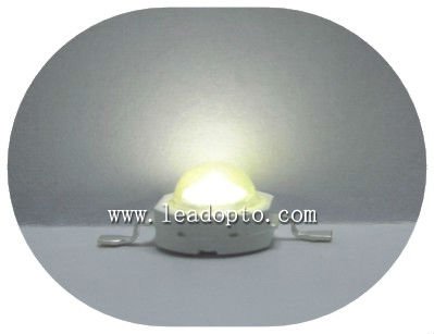
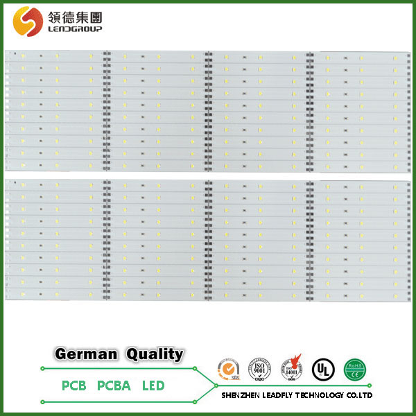
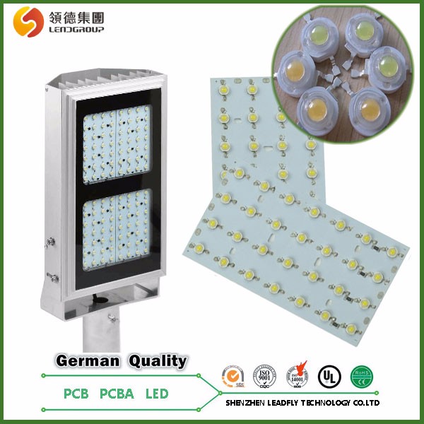
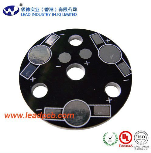
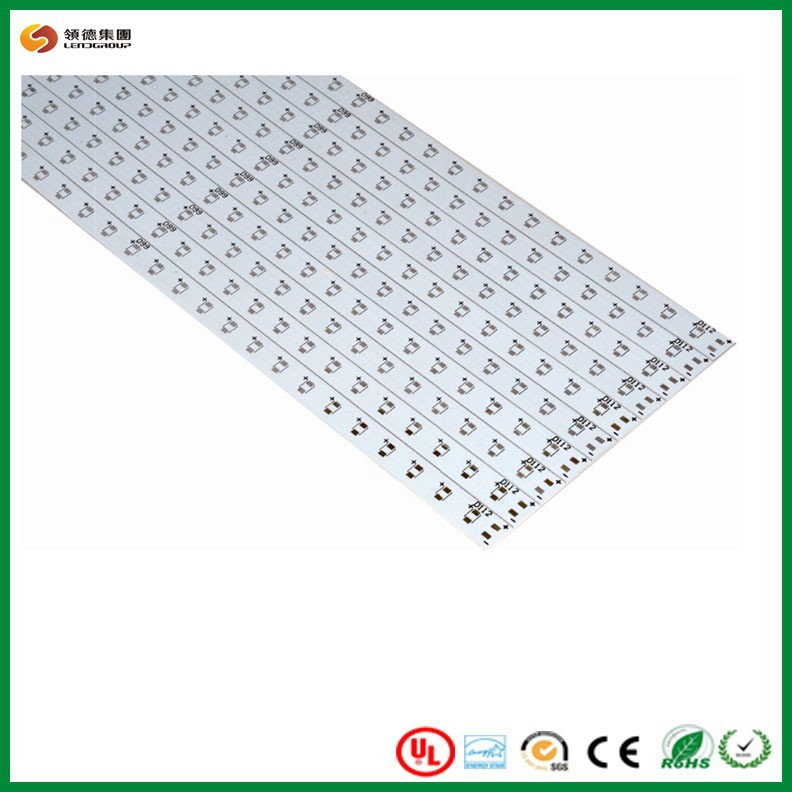
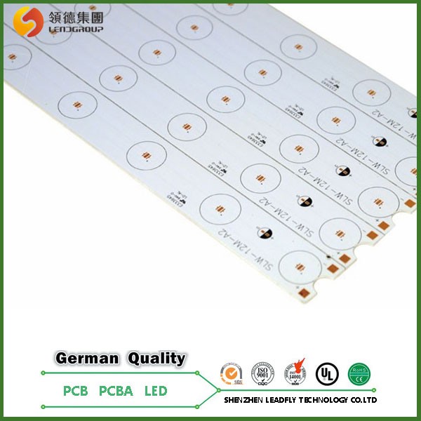
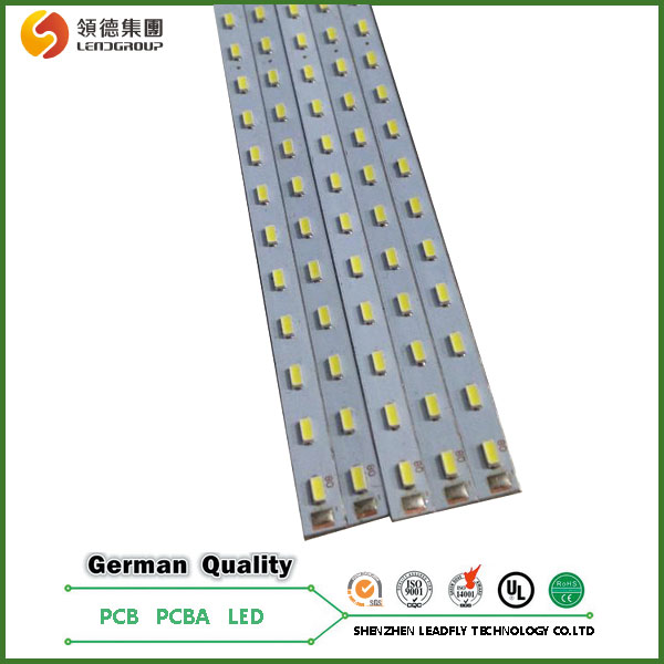
aluminum long led tube pcb,power led pcb made in China
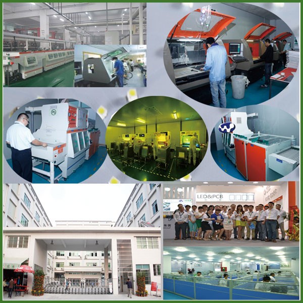
Company Information
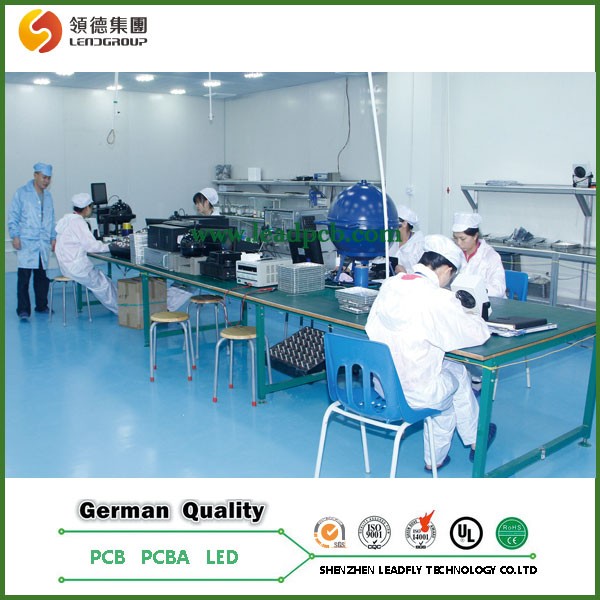
LEAD INDUSTRY LIMITED is an expert at PCB&PCBA, high power led,COB LED, SMD LED, SMT service manufacture, based in Shenzhen, Guangdong, China.
LEAD INDUSTRY LIMITED was founded in 2003,has two factory located in Shenzhen and Huizhou. We mainly offer Circuit Board manufacturing and OEM PCB Assembly Service, also with LED, all our product with CE&ROHS,UL: E333645, From our ISO9001 certified factory, we turn out up to 80000 square meter of PCBs monthly.
LEAD INDUSTRY LIMITED has a strong factory strength, supplier for GE,ABB,TCL,IKEA ect, which building a about 540000m2 industrial park in Jiangxi china.
Specification:
| Item | Specification | Remark | |
| Layer | 1-16 Layers | ||
| Material | FR-4, Aluminum, Ceramic based, Ployurethane/Mylar | ||
| Board Thickness | 0.04mm-3.2mm | Single FPC: 0.04mm (2mil) | |
| Mini. Core Thickness | 0.1mm (4mil) | ||
| Copper Thickness | Min. 1/2 oz, Max 4 oz | ||
| Min. Trace/ Spacing Width | 0.075mm (3mil) | ||
| Min. Hole for CNC Drilling | 0.25mm (10mil) | Laser Drilling: 0.1mm(4mil) | |
| Min. Hole for Punching | 0.7mm (28mil) | ||
| Dimension Tolerance | Hole Position | ±0.075mm (3mil) | |
| Trace Width | ±0.05mm (2mil) | ||
| Hole Size | PTH±0.15mm (6mil) NPTH±0.05mm (2mil) | ||
| Outline | Routing±0.15mm (6mil) Punching±0.10mm (4mil) | ||
| Bow and Twist | 0.7% —1.0% | ||
| Surface Finishing | Nickel/Gold Plating/ENIG/HAL | ||
| Insulation Resistance | 10KΩ - 20MΩ | ||
| Conductivity | <50Ω | ||
| Test Voltage | 300V | ||
| V-Cut | Panel Size | Min.110mm × 100mm, Max 660mm ×600mm | |
| Board Thickness | Min.0.6mm (24mil) | ||
| Temain Thickness | Min.0.3mm (12mil) | ||
| Tolerance | ±0.1mm (4mil) | ||
| Groove Width | Max.0.5mm (20mil) | ||
| Groove to Groove | Min.10mm | ||
| Groove to Trace | Min.0.50mm (20mil) | ||
| Slot | Slot Size Tol ≥2W | PTHL: ±0.15mm (6mil) W: ±0.1mm (4mil) | |
| NPTHL: ±0.125mm (5mil) W: ±0.1mm (4mil) | |||
Mini. Spaing between hole edge to circuitry pattern | PTH Hole: 00.13mm (5mil) | ||
| NPTH Hole: 0.18mm (7mil) | |||
Registration Tolerance of Front/Back image | Font image vs back image | 0.075mm (3mil) | |
| Multilayer | Layer-Layer misregistration | Max.4layers: 0.15mm (6mil) | |
| Max.6-16layers: 0.025mm (10mil) | |||
Min. spacing between hole edge to circuitry pattern of an inner layer | 0.25mm (10mil) | ||
Min. Spacing between board outline to circuitry pattern of an inner layer | 0.25mm (10mil) | ||
| Board thickness tolerance | 4layers: ±0.13mm (5mil) | ||
| 6-16lyaers: ±0.15mm (6mil) | |||
| Impedance Control | 60ohm ±10% | ||
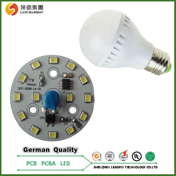
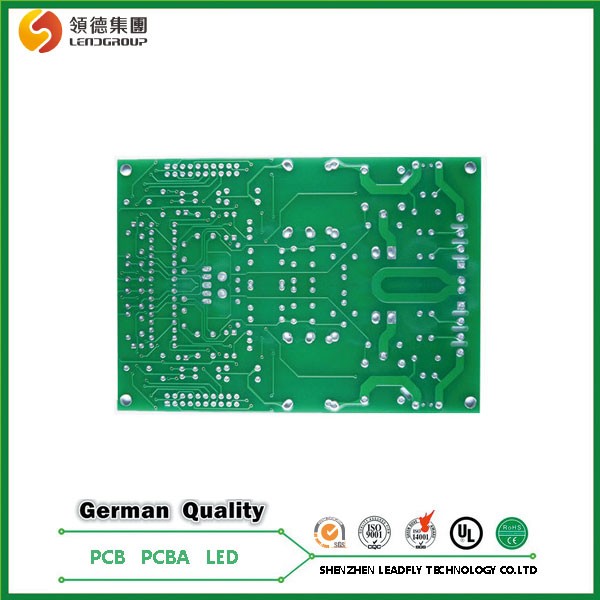
Product Description


FAQ
Q:Can you offer samples before mass production?
A: Yes, we can custom you sample to test before mass production
Q: When will I get the quotation after sent Gerber, BOM and test procedure?
A: Within 6 hours for PCB quotation and around 24 hours for PCBA quotation.
Q: How can I know the process of my production?
A: 7-10 days for PCB production and components purchasing, and 10 days for PCB assembly and
Testing
Q: How can I make sure the quality of my PCBAs?
A: We ensure that each piece of PCBA products work well before shipping. We'll test all of them according to your test procedure