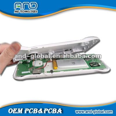

| 原産地: | 中国(本土) | 銘柄: | と | モデル番号: | 電子設計 | ブランド: | /oemodm | 表面仕上げ: | Hasl/鉛フリー/浸金等 | 認証: | Ul/rohs/ce/iso9001: 2008 | 基板材料: | Fr4/高tg | /pcbpcbaのプロトタイプ: | はい | 強力なソーシングコンポーネント: | はい | /pcbpcbaエンジニアリング実行: | はい | バックアップのサポート: | はい | 船積み: | /dhlフェデックス/ups/ems/tnt | アプリケーション: | 通信機器 |
包装
| 包装: | 標準パッケージ/odmパッケージ |
Our team can provide you with the support services you need to get your projects done - and on schedule!
Why choose ANDTech?
Our layout team can do a complete layout project or help with smaller portions such as placement studies, routing, generating proper manufacturing files, library management, and more. We are happy to make small changes or complete large complex designs.
We understand that our customers often need a PCB design completed quickly. We support our customers by providing expedited PCB layout service at no additional hourly cost.
We provide quotes on an hourly basis (time and materials) or with a fixed price. Call us today to find out how we can improve your design quality, meet your deadlines, and save money.
AND Technologies offers the fastest turnaround to reach the prototype stage, followed by quick transition to production and volume manufacturing.
Our engineer Team is professional and partner factory is highly equipped with advanced manufacturing facilities and machines. we can do for you at low cost but high quality.
- hardware design(circuit design ,PCB layout).According to custom-requirement
- software and firmware design, of MCU, DSP, embedded system ,ARM
- Mechanical design(2D,3D drawing),tooling and molding design
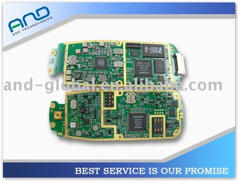
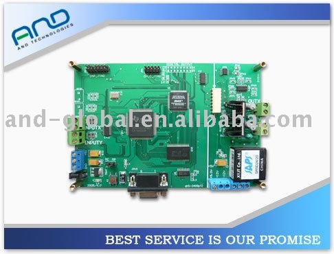
- integration and prototyping. finish a full-function products
- mass production and upgrade of existing designs
we will protect the intellectual property of the product for our customers.
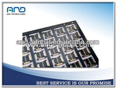
Mass production is the production of large amounts of standardized products, including and especially on.
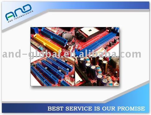
- High-Density BGAs, QFNs, Micro-Vias, Ultra-Fine Trace and Space
- Hand-Crafted Layout for Memory Systems, Chipsets, High-Speed Designs
- Layout Planning for High-Current Applications (Power Supplies, Motor Control) Minimizing Current Loops
- RF Layout Strategies
- Design for EMI Compliance
- Design for Manufacturability Stack-Up, Spacing, IPC Footprints
- Specialty Design Considerations
- Controlled Impedance
- High-Speed PCB Materials
- Blind and Buried Vias Thermally Conductive PCB Materials
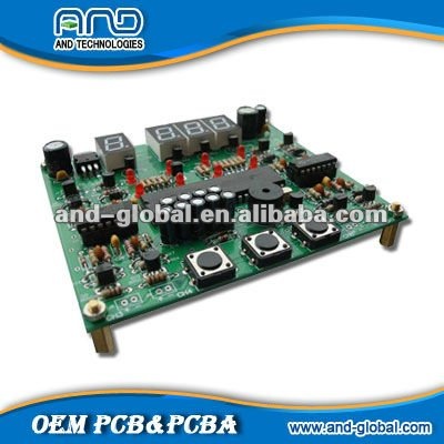
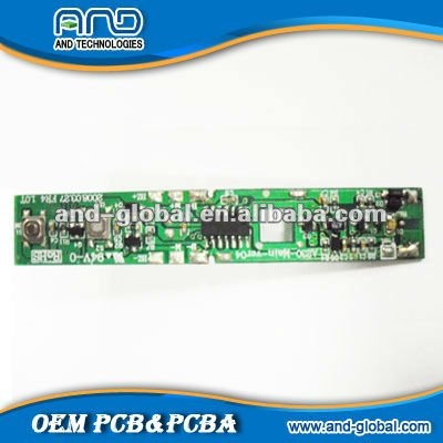
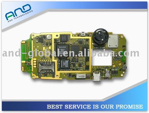
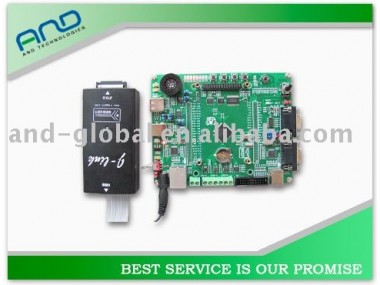
- Electronic design about motor driver,PCB Layout Design,Circuit Design,SMT,schematics design,Technical support
Thanks for your dropping by! Please let me know what you think of the electronic design!
For over 8 years PCB Assembly has been delivering superior quality and on-time delivery to its customers.
We will handle your order with the greatest care and responsibility. Give us a try, you will be happy you did!

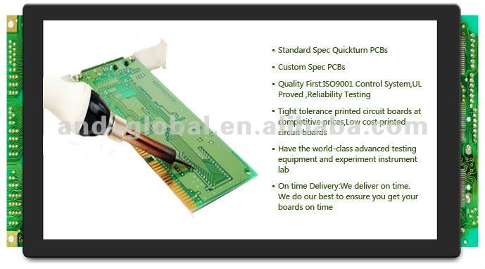
Our Factory Manufacture Capability
Item | Manufacture Capability |
Board Material | FR-4 |
Layer | 1-20 |
Finished Board thickness | 0.2 mm-3.8mm ( 8 mil-150 mil ) |
Board Thickness Tolerance | ±10% |
Copper thickness | 0.5 OZ--2.0OZ |
Impedance Control | YES |
Hole tolerance | PTH:±0.075mm NPTH: ±0.05mm |
Min drilled Hole size | 0.15mm(6mil) |
Min Laser hole size | 0.1mm(4mil) |
Min Space Width | 0.075mm (3 mil) |
Min Trace Width | 0.075mm(3mil) |
BGA Pitch | 0.2 mm (8 mil) |
Solder mask Color | Green , Red , Blue , Black , White |
Panel Outline Tol (+/-) | CNC: ±0.125mm, Punching: ±0.15mm |
Surface finish/treatment | HASL/HASL lead free , Immersion Gold |
Certificate | ROHS, ISO9001:2008, SGS, UL certificate |